Have you ever wondered how the electronics in your smartphone, car, or even medical devices work?
The answer lies in a small but crucial component: Printed Circuit Boards (PCBs). These boards are the backbone of nearly every electronic device, ensuring everything runs smoothly, from your daily gadgets to cutting-edge space technology.
In this article, we will closely examine how those components are manufactured and tested to perform flawlessly.
Manufacturing and Testing of PCBs
Manufacturing PCBs is a multi-step process that requires precision, consistency, and technological expertise. The predefined design is transferred to the conductive copper layer by printing the PCB layers. Then, tiny holes are drilled into the board, allowing components to be mounted. The holes are then plated with copper to create electrical connections. A protective layer called a solder mask is applied to get the board ready for soldering.
Soldering is a critical process that connects all the components to the board, ensuring they communicate effectively. Depending on the complexity and type of PCB, the soldering can be done via different methods, including wave soldering, reflow soldering, or manual soldering. Any imperfections in the soldering process—such as cold solder joints, bridging, or voids—can lead to serious performance issues for the end device. This leads to the final step of manufacturing, testing and inspection.

After the PCB is assembled, it undergoes rigorous testing to catch any potential defects. One standard method is using X-rays, which allow manufacturers to inspect the board without damaging it. Manufacturers can, this way, inspect and verify that solder joints are secure and there are no hidden issues that could cause problems later on.
The Future of PCB Testing
As the PCBs themselves are undergoing constant development for more and more advanced applications, the testing must keep up the pace. Although 2D X-ray quality control has become a standard part of manufacturing processes, it cannot catch every issue. Some defects appear only after the device with PCB is in use when it’s exposed to heat or other stresses. These hidden defects can lead to device failures after they’ve already reached customers.
Therefore, manufacturing companies aim to find a solution for internal quality control that ensures the detection of all production defects, thereby preventing faulty products and reducing costs associated with product recalls and market withdrawals.
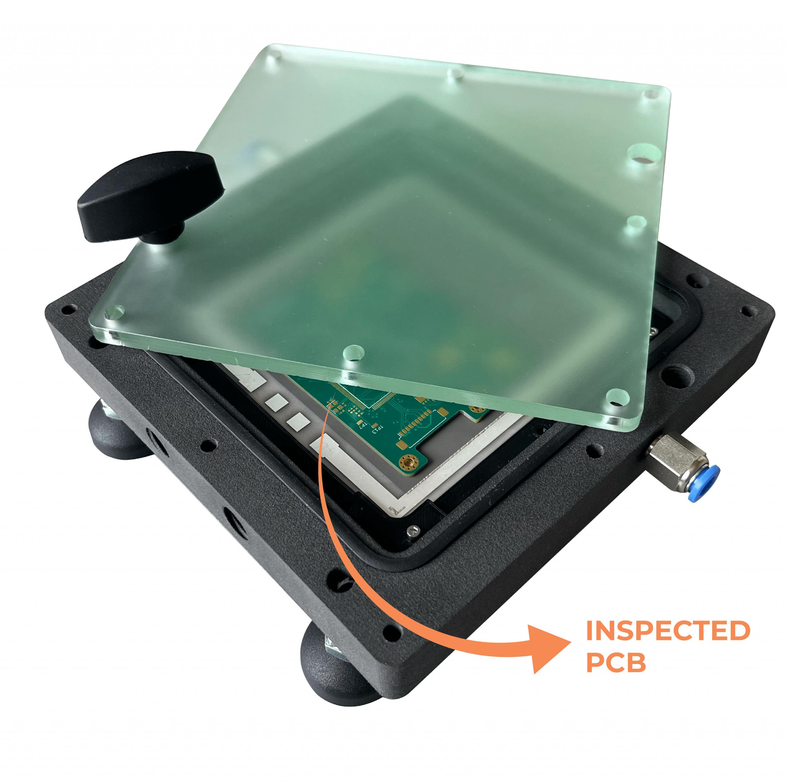
CactuX introduced In-situ soldering BOX for 2D X-ray systems.

CactuX aims to expand the possibilities of 2D X-ray systems with its new In-situ BOX specifically designed to test solder joints. A tool that enhances traditional 2D X-ray systems by allowing real-time monitoring of the soldering process. This add-on simulates the exact conditions under which soldering happens, such as temperature changes, so manufacturers can watch for defects as they form.
This technology helps manufacturers pinpoint issues like void formation and understand how materials behave during soldering. As a result, companies can improve their soldering techniques, making electronic components more reliable and durable.
CactuX In-situ soldering BOX reveals new and deeper information about PCB functionality for the manufacturers.
Interested in exploring how CactuX In-Situ Soldering BOX can improve your soldering process and PCB quality? Our team is ready to discuss your specific needs, provide technical advice, or schedule a demo measurement. Contact us today to discover how our solutions can help you.


This project is co-funded by the European Union.
Project name: Development of a heating element in thick film technology on AlN substrate (Vývoj topného tělesa v tlustovrstvé technologii na AlN substrátu)
Project goal: The main objective is to complete the development of a special product that enables high-precision quality control of solder joints using X-ray imaging
Registration number: CZ.01.01.01/05/23_009/0003367
Place of implementation: Hlavní 683/104, Lelekovice, 664 31 Brno-venkov
Operational Programme Technology and Applications for Competitiveness (Operační program technologie a aplikace pro konkurenceschopnost)
Provider: Ministry of Industry and Trade CZ (Ministerstvo průmyslu a obchodu)